
Aligned 2-Photon Lithography
3D printing with automatic alignment and nanoprecise 3D positioning on complex substrates such as optical fibers or photonic chips opens up new possibilities for 3D nano- and microfabrication.
Basics and principles
Aligned 2-Photon Lithography
as a powerful solution for on-fiber printing
Aligned 2-Photon Lithography (A2PL®) is Nanoscribe’s new proprietary nano- and microfabrication technology based on Two-Photon Polymerization (2PP) that automatically aligns printed structures on optical fibers and photonic chips, e. g. as optical interconnects for photonics packaging. High-precision detection systems enable the identification of fiducials or topographical substrate features, ensuring highly accurate alignment for 3D printing.
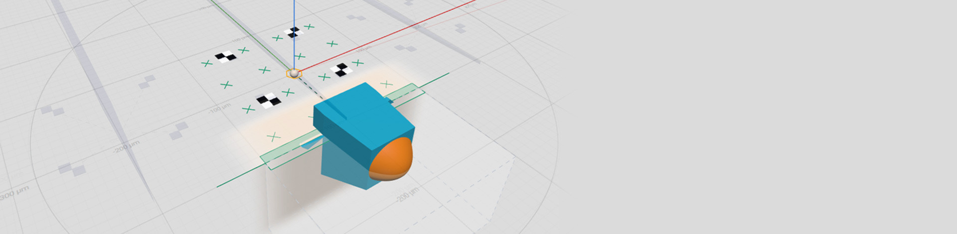
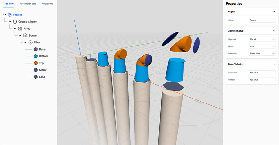
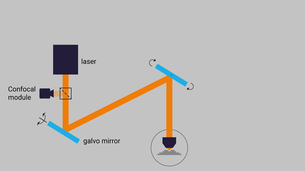
A2PL works with nanoPrintX, a software tool based on a scene graph concept to define print projects for aligned 3D printing. The tree-like data structure provides a hierarchical organization of all print-relevant objects and operations to define what, where, in which spatial orientation and how to print. Individual alignment markers as well as substrate features such as chip edges and fiber facets can be defined in nanoPrintX. Using Quantum X align's confocal unit or fiber illumination unit, these specific substrate markers can be identified and matched to the digital model defined in nanoPrintX. The Quantum X align system is equipped with both Aligned 2-Photon Lithography and nanoPrintX by default.
Then, the position of the fibers is detected with submicron accuracy and compensated for smallest substrate tilts during the print in all spatial directions. For this, the system identifies the illuminated fiber core and marks the center of the core as the origin of a virtual coordinate system to which the print object is aligned. The virtual z-axis and its orientation in space is determined by moving the substrate downwards and identifying the position of the fiber core on multiple positions along this vertical movement of the stage. As a result, the optical axis orientation is detected and set as the virtual z-axis for a tilt-compensated nanofabrication of microoptics along the optical axis with submicron precision.

Aligned 2-Photon Lithography
for aligned 3D printing on photonic chips
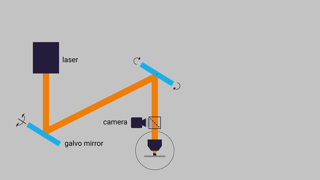
To detect substrate topographies, a high precision confocal detection module maps the surface. This module is integrated into the beam path of the near-infrared printing laser, which scans over the sample surface. The back-scattered light is then confocally detected by the system to record high resolution 3D topographies while moving the stage vertically. Marker recognition is achieved by taking an image at a single z-position in combination with a pinhole spatial filter, resulting in a lateral detection accuracy down to 100 nm. Thus, the confocal module measures real 3D topographies and is much more accurate than image-based measurements using the system camera.
Printing on the surface of a photonic chip
Accurate alignment of optical components on a photonic chip, e.g. as optical interconnects for photonics packaging, is achieved with high-resolution 3D topography mappings provided by the confocal unit. In the nanoPrintX software, you can add the chip layout and alignment markers to the print job. The nanofabrication system detects the markers and matches them with the print job to determine the exact position and orientation of, for example, the waveguides of a photonic chip. This ensures 2PP-based 3D nanofabrication of microoptical elements and interconnects with best optical performance and minimized coupling losses, enabling efficient light coupling through Free Space Microoptical Coupling (FSMOC) as a powerful solution for photonics packaging.
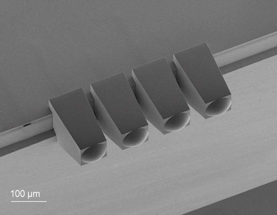
Printing on the facet of photonic chips
The printing workflow on the facet of a photonic chip includes edge detection by the confocal detection module. Adding edge detection as an alignment node in nanoPrintX enables the definition of the edge or the confocal scan area where the system should scan for it. Then, the 3D nanofabrication system’s confocal detection module takes an image stack at the defined position and identifies the edge.
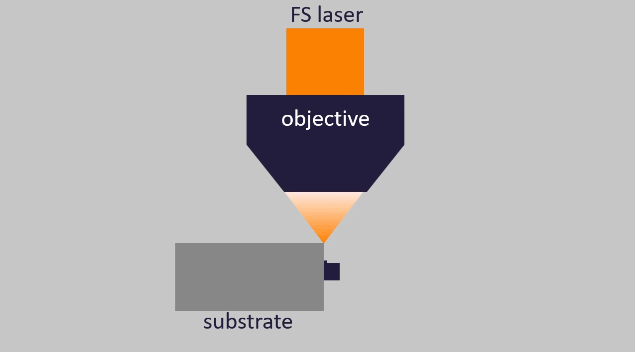
Printing onto a chip’s facet from the top, i.e. perpendicular to the substrate surface, is a challenging task. It requires a precise positioning system and printing solutions to overcome the “shadowing effect”: This effect occurs because a substantial part of the intensity in the focal point of the printing laser is lost when printing onto a facet. This is due to the light being partly blocked by the edge of the substrate. The shadowing effect is more prominent near the substrate wall, which requires higher exposure doses. The A2PL® nanofabrication system automatically compensates for this effect using a proprietary process and dynamically adjusts the exposure conditions during printing. A2PL® is subject to Nanoscribe’s proprietary intellectual property. As a result, microoptics and other print objects are written onto the facet of a substrate with submicron shape accuracy by Two-Photon Polymerization (2PP) and A2PL® technology.
Related product
Quantum X align
Connect to the photonic world
Aligned 3D printing.
The Quantum X align system is designed to automatically align printed structures on optical fiber cores and photonics chips using the advanced A2PL® technology.
